CALLISTO Receiver Testing
CALLISTO Receiver printed circuit boards (PCB) in Partially-Built and Ready-Built versions are initially tested on a laboratory test fixture. The test fixture is supplied by 28 Vdc, which may be used to power an external noise source through a "hot/cold" switch and BNC connector. It also powers a small step-down linear power supply mounted inside the test fixture chassis. This power supply is adjusted to 12 Vdc for powering the PCB. The test fixture also provides a DB9-F connector for the EIA-232 interface. Click here for layout and schematic drawings associated with the test fixture.
For the Partially-Built version, the PCB is installed on the test fixture for preliminary as well as final testing. For the Ready-Built version, the PCB is installed on the test fixture for preliminary testing and then installed in the enclosure for final testing with a different test fixture shown below. The PCBs and Receivers are tested according to the procedures given in the CALLISTO Construction Manual.
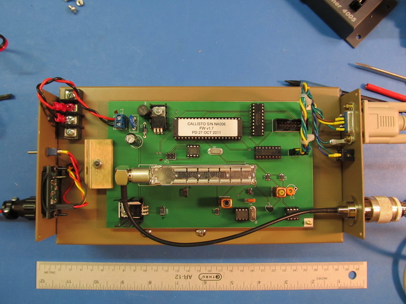
The picture immediately below shows a completed PCB in-place for testing. An annotated view of the test fixture alone is provided below.

The ready-built and tested versions of the Callisto are tested using automated software procedures and the test fixture shown below.


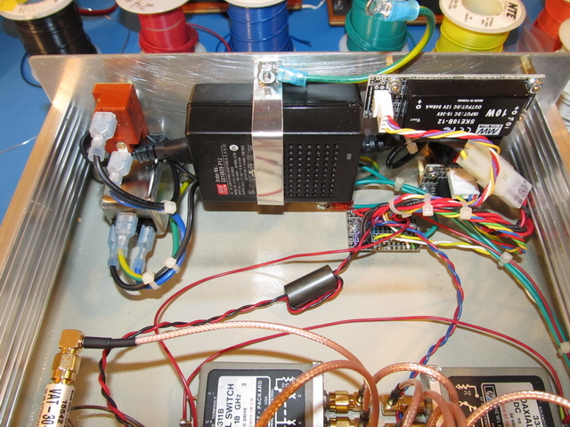
Interior views of test fixture below. The object at the lower-right is a USB-controlled frequency synthesizer before the cover was placed on its enclosure.